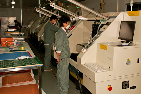
We specialise in providing prototye and small batch PCBs for fabrication.
Below are some image for manufacturing process,including,drill,plating and final
Fabrication.all our PCB go through intensive testing and quality control during
Each step of the manufacturing process.
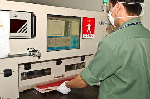
Inner layer core shown after etch\dryfilm strip processes have been completed.
The core is now ready for post etch punch.
Punching core material is the only acceptable method of building precision tooling which must remain accurate
in a production atmosphere.
CNC machines are complete with drill and profile routing software allowing
for high performance and throughput.

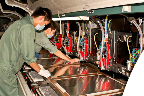
Strip-Etch-Strip Line
Production panels proceed to etching to remove unwanted copper and into the strip line
to remove protective film.
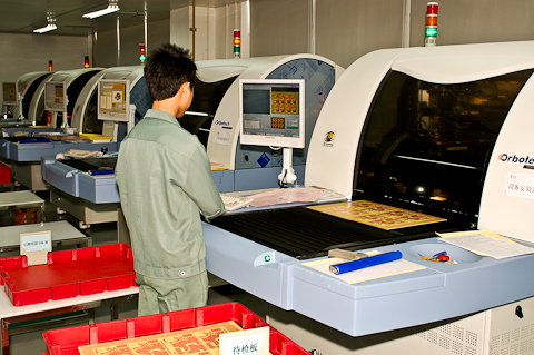
Automated Optical inspection(AOI)
Using the latest in optical inspection equipment on internal and external
layers allows for minimal fallout on final product
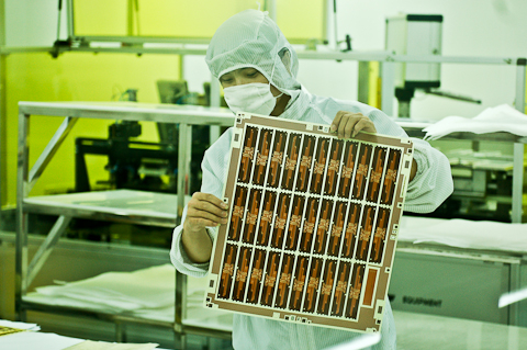
Final Fabrication Routing&Scoring
 IblueBoard specializeds in PCB prototpe, medium volume to mass production with Quick turn...